SolVisionCase Study
Detecting Adhesion Defects in Semiconductors
AI deep learning technology for visual inspections
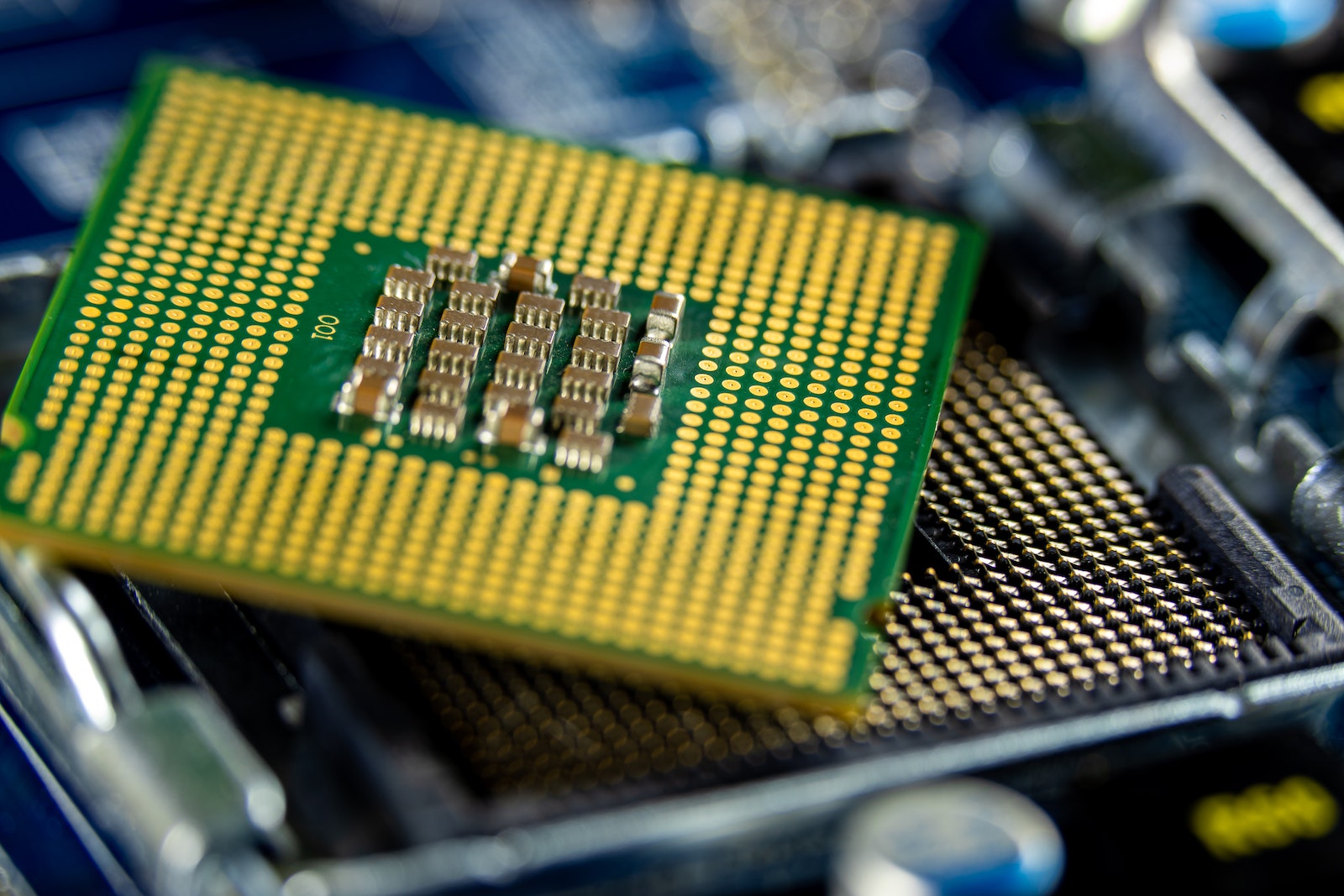
Die bonding technique and product stability
Die bonding (also die mounting) is a key step in manufacturing semiconductors and involves connecting the silicon chip to a lead frame using die attach adhesive, in order to form a thermal or electrical path. One of the biggest challenges of die bonding lies in how to fix the chip onto the lead frame using the least amount of adhesive. Excessive adhesive may remain on the chip or overflow on the circuit board and cause the chip to tilt, affecting stability of the whole semiconductor package.
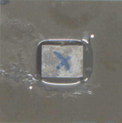
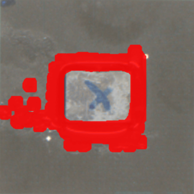
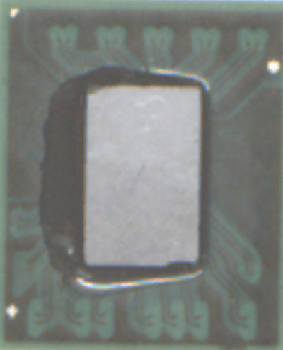
Irregular defects: light refraction, overflowing and excessive adhesion
Die attach adhesives are transparent, and cause light to refract which impacts detection rates. Overflowing and excessive adhesion defects are usually unsystematic and do not have fixed positions or shapes. Random production errors like these make it difficult for traditional inspection systems to establish rules for effective detection.
AI feature learning and data augmentation
Based on AI deep learning, SolVision is capable of accurately identifying random and complex defects. The software’s Segmentation tool uses sample images to build an AI model for recognizing the features of varying defects to locate them. For improved detection rates, the data augmentation function allows simulation of potential faulty product scenarios, allowing the AI to expand its knowledge of defect characteristics. Increasing the dataset strengthens the system’s recognition ability so that the inspection process becomes less affected by external factors.
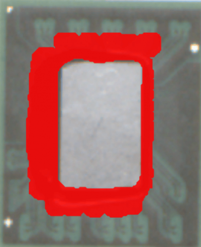
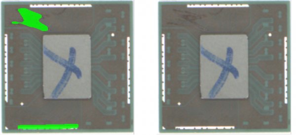
AI Inspection
Original
Result
Original
Result