Semiconductors

  • AI Inspection for Semiconductor Components

    Overcoming traditional AOI limitations, Solomon’s SolVision quickly performs OCR without being affected by background or lighting conditions, complexity, or appearance of the serial number.

  • Close up epoxy stamping on lead frame in die attach machine in semiconductor manufacturing.

    Automating Quality Inspection of Lead Frames

    As semiconductor manufacturing becomes more sophisticated, the process of creating lead frames needs to improve in accuracy and yield.

  • Detecting Adhesion Defects in Semiconductors

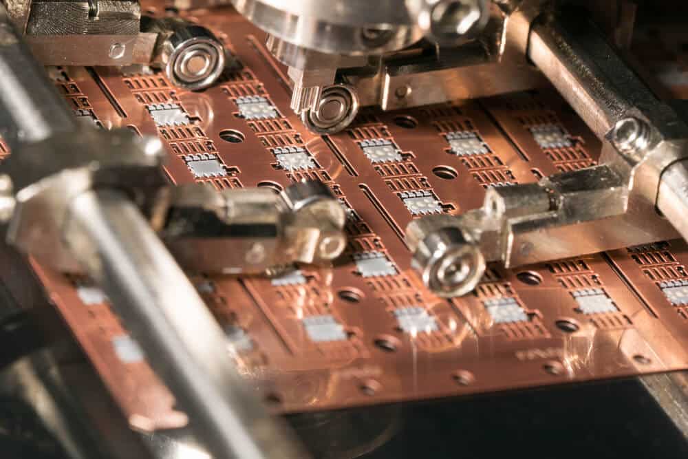
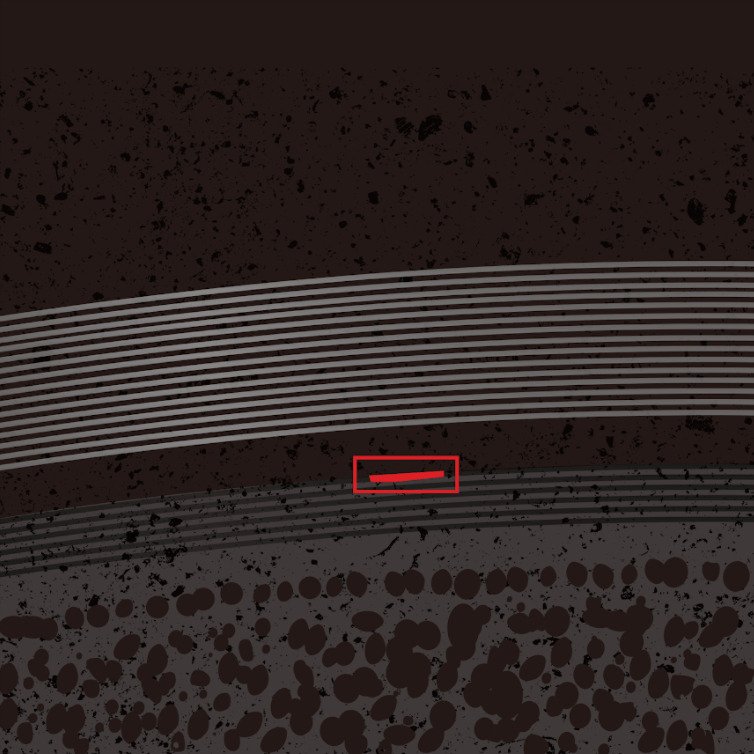
    Excessive adhesive may remain on the chip or overflow on the circuit board and cause the chip to tilt, affecting stability of the whole semiconductor package.

  • Two scientists in sterile suits inspecting a silicon wafer removed from a soldering jet printer in a semiconductor production facility.

    Automating Semiconductor Wafer Inspections

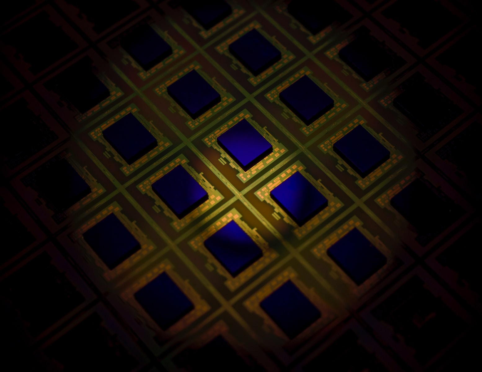
    Faulty wafers also usually have subtle defects randomly scattered on the surface, and this prevents AOI systems from setting rules for efficient inspections.

  • Central Processor Of A Computer

    Inspecting Semiconductor Packaging Processes

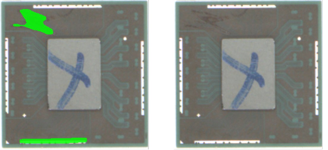
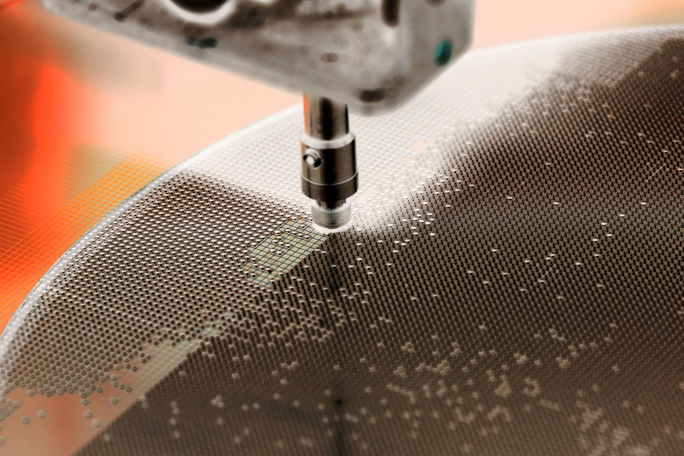
    SolVision enables visual inspection through AI image analysis, strengthening the reliability of displacement and angle information to recognize defective products and errors in the die bonding process.

  • Quality Control of Wafer Dicing

    Using SolVision’s Instance Segmentation tool, irregular lines and multi-drilling defects are labeled in sample images to train the AI model.

  • a group of square objects

    Detecting Chipping Defects in Wafer Dicing

    The location, size and shape of cracks vary each time, and traditional optical inspection cannot accurately identify such unpredictable defects.

  • Inspecting Packaged Semiconductor Chips

    The Anomaly Detection tool uses deep learning technology to teach the AI model sample images of “perfect” wafers.