SolVisionCase Study
Detecting Chipping Defects in Wafer Dicing
Quality control of semiconductor die with AI
Reducing semiconductor wafer size
Wafer sawing helps singulate the wafer into individual die for subsequent processing. As modern electronics require thinner, smaller, and lighter wafers, shrinking wafer chips require more meticulous cutting processes. Cutting pathways are narrowed, the silicon crystals become more fragile, and sawing-induced damages are more prevalent.

Unpredictability of die edge cracking
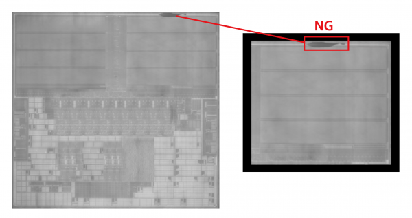
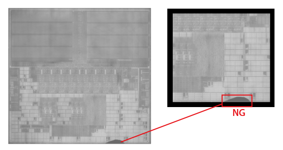
Cracked edges caused during wafer dicing damages the strength of the wafer. In severe cases, it may lead to breakage when the chip is stressed in subsequent production processes. The location, size and shape of cracks vary each time, and traditional optical inspection cannot accurately identify such unpredictable defects.
Laying foundations for packaging with AI
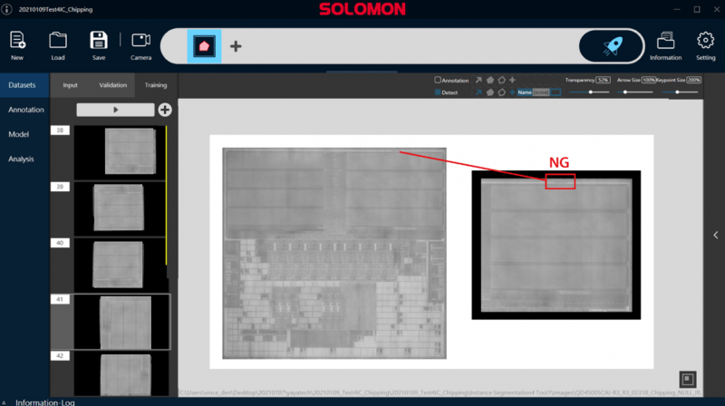
Offering superior recognition, SolVision can train an AI model capable of inspecting wafers and recognizing production defects through image processing. The system allows different variations of chipped edges to be automatically detected and located in real-time, greatly reducing the possibility of breakage in later packaging processes.
AI Inspection
Cracked edges

