BGA Soldering Inspection Using AI
The Case
Accurate BGA Soldering Inspection
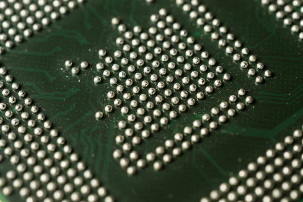
Ball Grid Array (BGA) packaging is widely used in high-density semiconductor designs to improve electrical reliability and minimize shorts. Electrical connections are formed through an array of solder balls on the underside of the package, enabling compact interconnects between the BGA and the PCB.
Plastic BGAs with laminated substrates are common in high-volume manufacturing. During reflow soldering, thermal stress and temperature variation can deform the PCB or package, causing defects such as non-wetting, solder ball overlap, cold solder joints, and voids. These defects can lead to short circuits or reduced connection reliability, making accurate BGA soldering inspection critical.
The Challenge
Inspecting Hidden BGA Solder Joints
Traditional optical inspection cannot evaluate BGA solder joints located beneath the package. X-ray inspection is required to detect internal defects; however, X-ray images often have low contrast and high background noise.
Rule-based inspection systems struggle under these conditions. Variations in solder shape and density reduce detection reliability and increase false positives, limiting inspection effectiveness in production environments.
The Solution
SolVision AI BGA Soldering Inspection
SolVision uses deep learning to analyze X-ray images for BGA soldering inspection. The AI model is trained with labeled defect data, including non-wetting, solder ball overlap, size deviations, and short circuits.
The model identifies subtle defect patterns in noisy, low-contrast images that traditional algorithms cannot reliably detect. With SolVision, inspection consistency improves while false positives are reduced, supporting stable inline quality control.
BGA Soldering Defect Classification

OK: Acceptable solder joint

NG: Defective solder joint

Wrong Size: Abnormal solder ball dimensions

Short Circuit: Electrical bridging between solder joints