CMP Quality Inspection Using AI
The Case
Ensuring Surface Quality in CMP Processes
Chemical Mechanical Planarization (CMP) is a critical step in semiconductor manufacturing that planarizes wafer surfaces and removes excess material between process layers. Each wafer must undergo CMP to achieve the surface uniformity required for subsequent lithography and deposition steps.
However, the CMP process can introduce surface defects such as scratches, particle contamination, and slurry-induced damage. These defects can impact device performance and yield, making reliable quality inspection essential for maintaining wafer integrity.
The Challenge
Detecting Subtle Defects on Complex Wafer Surfaces
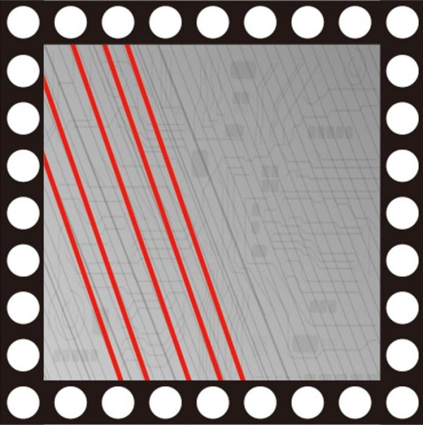
CMP-induced defects such as fine scratches, particle residue, and polishing pad debris are low-contrast and spatially non-uniform, making them difficult to isolate on wafer surfaces. CMP processing also generates shallow polishing traces that produce complex, non-uniform background textures in inspection imagery.
Rule-based AOI systems are limited in handling variability in defect morphology and wafer surface appearance, particularly under low signal-to-noise conditions. As a result, conventional inspection approaches are insufficient for robust CMP quality inspection in high-precision semiconductor manufacturing environments.
The Solution
SolVision AI CMP Defect Inspection
SolVision applies AI vision inspection to detect CMP defects on semiconductor wafers.
Using deep learning, the system is trained with sample images in which defects such as fine scratches and particles are labeled. The AI model learns to distinguish defect features from complex wafer backgrounds, enabling reliable detection under challenging inspection conditions.
The AI vision system identifies:
- Fine surface scratches
- Particle residue and contamination
- Polishing pad debris and surface anomalies
SolVision AI-based inspection enables precise defect detection and localization, including defect position and size. Continuous learning further improves detection performance, supporting consistent and reliable CMP quality inspection.
Wafer Surface Defect Detection


CMP-induced wafer surface defects
AI wafer surface defect detection