
SolVisionCase Study
BGA Soldering Inspection Using AI
Case
Accurate BGA Solder Inspection
Ball grid array (BGA) technology is a preferred packaging method for high-density and advanced semiconductor chips, designed to reduce electrical shorts and enhance overall reliability. This approach uses an array of small solder balls on the underside of the package to create high-density electrical connections between the BGA and the PCB. Plastic BGAs, commonly using laminated substrates, offer a cost-effective solution for high-volume manufacturing, especially in consumer electronics and other cost-sensitive applications. However, during the reflow soldering process, temperature variations can cause PCB and BGA deformation, leading to defects such as non-wetting, solder ball overlap, cold solder joints, and voids—all of which can result in short circuits or weakened connections. Precise inspection is critical to ensuring the reliability and functionality of the final product.
Challenge
Achieving Precision in BGA Defect Detection
Traditional optical inspection methods are often insufficient for verifying soldering quality in BGAs, particularly for the dense array of solder balls on the bottom surface. X-ray imaging is crucial for penetrating the package and detecting potential soldering defects hidden beneath the surface. However, X-ray images often suffer from significant background noise and lack clear contrast, making it challenging for rule-based systems to accurately detect defects and assess soldering quality.
Solution
AI-Driven Defect Detection for BGA Soldering
SolVision leverages deep learning to train its AI model using labeled sample images of soldering defects, such as non-wetting and solder ball overlap. By harnessing advanced AI algorithms, SolVision not only identifies these defects with high precision but also significantly speeds up the inspection process, ensuring quicker and more reliable quality control. The model is trained to recognize subtle defects even in noisy and low-contrast X-ray images, a challenge that traditional inspection systems struggle with. This results in accurate defect detection that enhances inspection reliability and minimizes false positives.
BGA Soldering Defect Detection
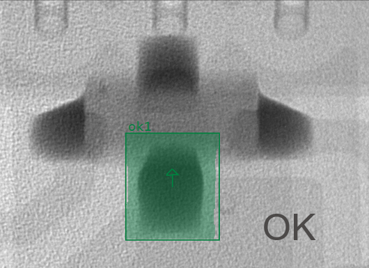
OK
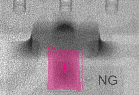
NG
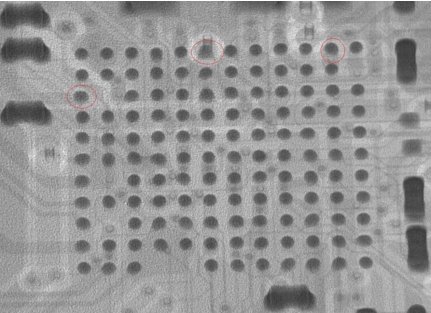
Wrong Size
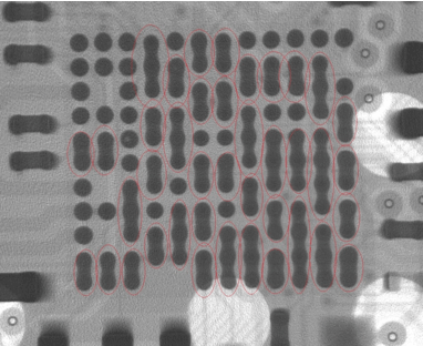
Short Circuit