SolVisionCase Study
Automating Semiconductor Wafer Inspections
Intelligent AI defect detection for silicon wafers
Balancing yield and quality of silicon wafers
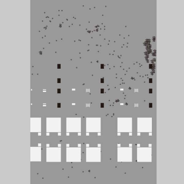
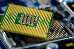
During production, semiconductor wafers undergo processes such as lithography, etching, film deposition, diffusion, and grinding, and are exposed to different substances in the environment that can cause quality affecting defects. Lasers can be used to repair silicon cells with certain defects yet this is an inefficient step for wafers with too many defects, as they are better off eliminated directly to avoid slowing down production. An inspection process is necessary to locate defective wafers suitable for repair.
Rigid traditional inspection systems
Traditional rule-based systems are easily influenced by external lighting conditions and unable to classify full frame images, so excessively damaged wafers cannot be eliminated in the preliminary stage. Faulty wafers also usually have subtle defects randomly scattered on the surface, and this prevents conventional vision systems from setting rules for efficient inspections.
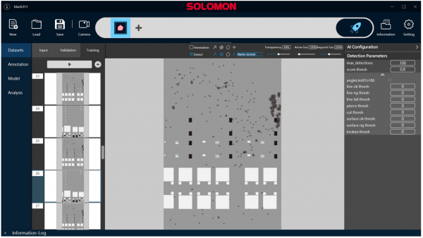
Flexible defect detection with SolVision
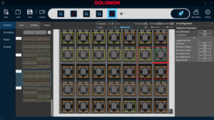
Powered by AI, SolVision is capable of recognizing the features of different defects and identifying substandard wafers. First, the system uses the Classification tool to determine whether a wafer has been damaged beyond repair. Image processing then divides scanned images of wafers into sections, and the Segmentation tool inspects them for defects thoroughly. Information such as defect characteristics, location, size and other data are recorded to improve the efficiency of subsequent repairs.
AI Inspection
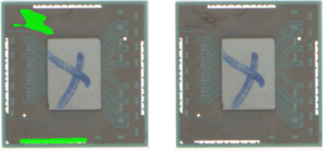
Golden Sample
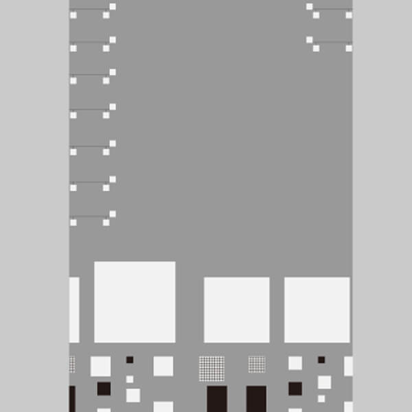
Defective Product