SolVisionCase Study
Inspecting Semiconductor Packaging Processes
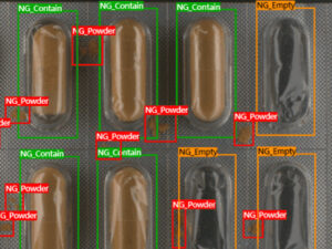
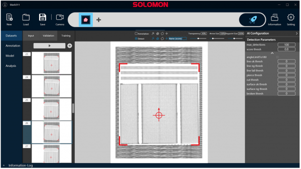
Advanced AI defect detection technology
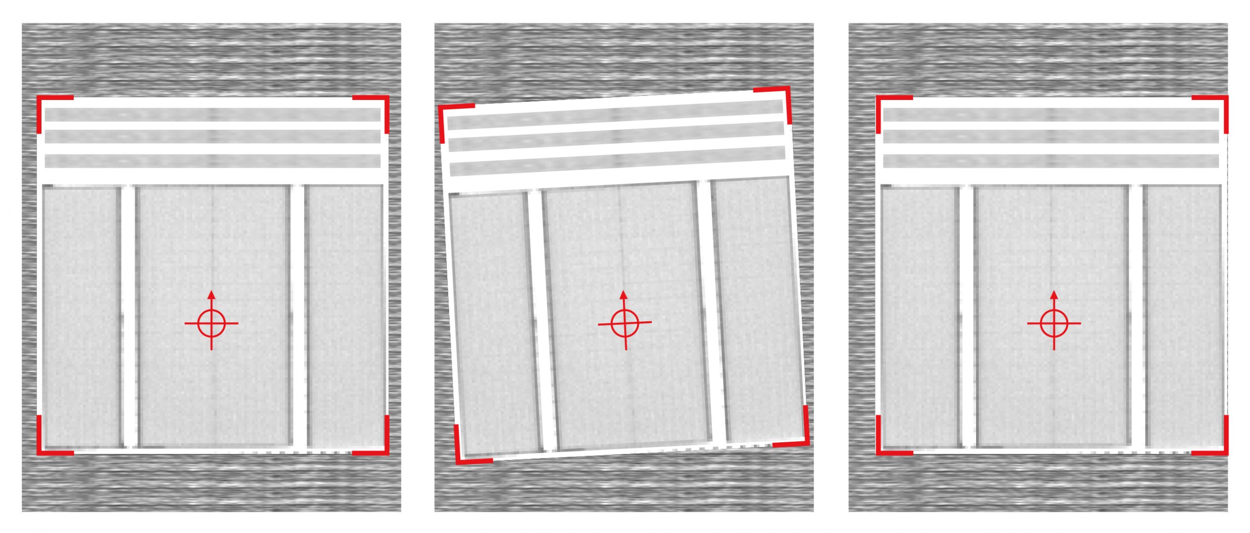
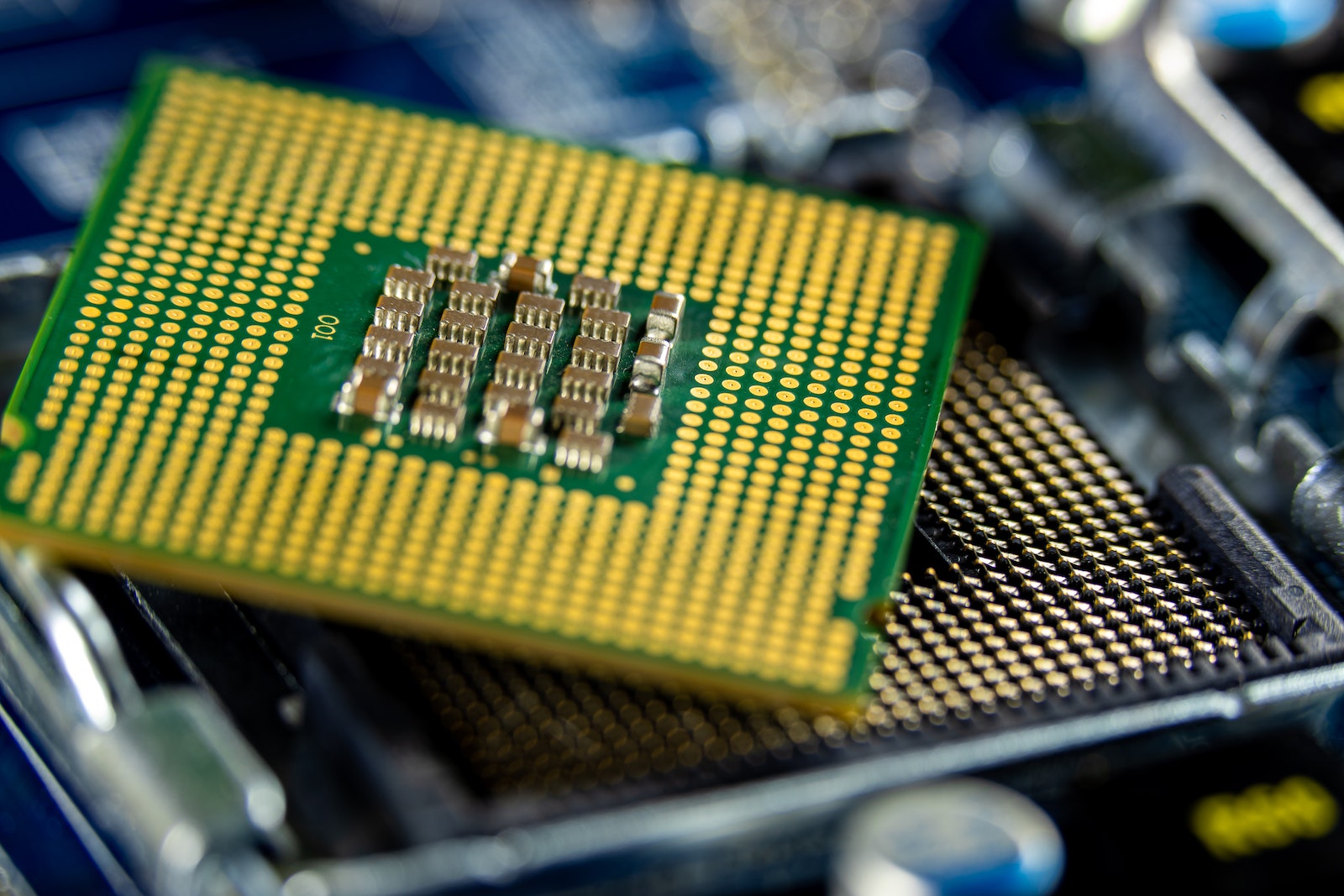
Semiconductor die bonding process
Die bonding (or die mounting) is an important step in semiconductor packaging, which requires adhesion of the silicon chip to the lead frame to form a thermal or electric path. As such, the accuracy of the die bonding process is key to the quality and yield of semiconductors.
The weaknesses of conventional inspections
Die bonding is a priority when packaging semiconductors, and the execution requires exceptional speed and accuracy. Because of the complexity of captured images, rule-based vision systems often cannot establish rules to flexibly detect a high number of random defects, such as in this case angle or position deviations, misshapen or missing components. Missed inspections and misjudgments are inevitable, and affect the productivity of the packaging process.
AI optimization of semiconductor packaging processes
SolVision enables visual inspection through AI image analysis, strengthening the reliability of displacement and angle information to recognize defective products and errors in the die bonding process. Additionally, the AI model can absorb data about different chip structures and extend inspections to multiple types of semiconductor packages.
AI Inspection
Golden Sample
Angle deviation
Displacement