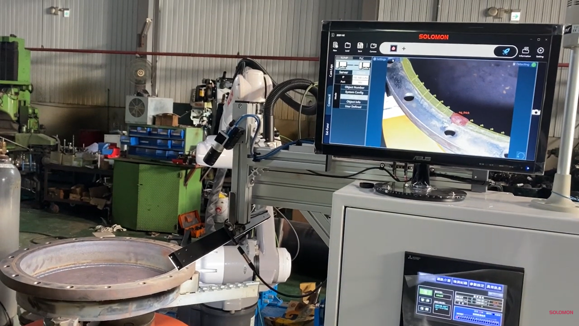
SolVision AI detects BGA soldering defects, improving inspection consistency, accuracy, and inline quality control in PCB and semiconductor production.
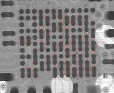
SolVision AI enhances Multilayer Ceramic Capacitor (MLCC) defect detection, reducing false rejections and improving quality control in electronics production.
SolVision enhances cookies quality with AI-powered quality inspection, ensuring consistent appearance and high detection accuracy in snack food production.
SolVision’s AI and OCR technology enhances Tire Identification Number inspection, improving accuracy, efficiency, and quality control in tire production.
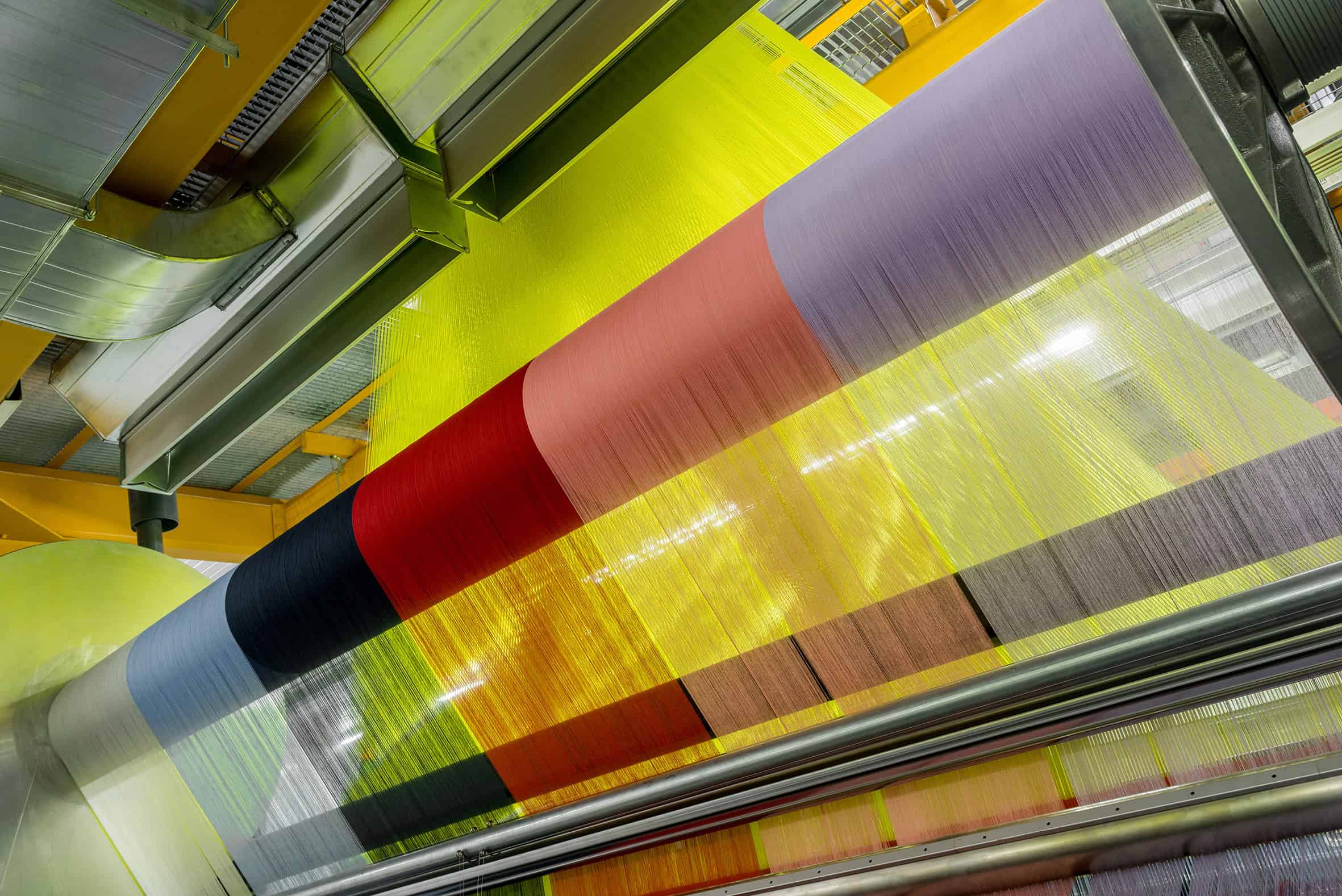
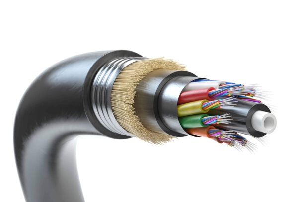
SolVision AI enhances cable defect detection, improving cable insulation quality control, inspection accuracy, and production efficiency for wires and cables.