SolVisionCase Study
AI Inspection Solution for Semiconductor Wafers
Quality control of chemical mechanical polishing (CMP) processes
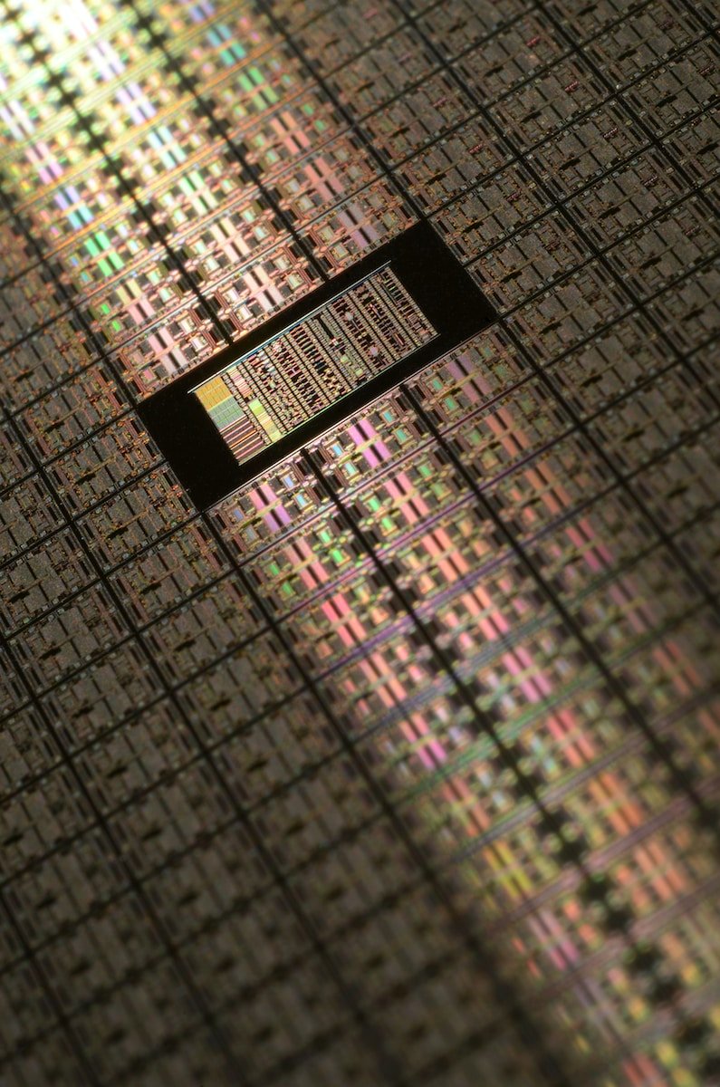
CMP and wafer surfaces
Chemical Mechanical Planarization (CMP) is an indispensable process in semiconductor manufacturing, and its purpose is to rectify small defects created in previous production steps. Each wafer layer needs to be polished and have all excess materials removed from its surface by CMP before the next layer can be made. However, excessively large particles and abrasions from the slurry may cause small scratches on the wafer, which are the most common type of defect caused by CMP processes.
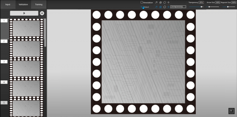
Complex backgrounds and subtle wafer defects
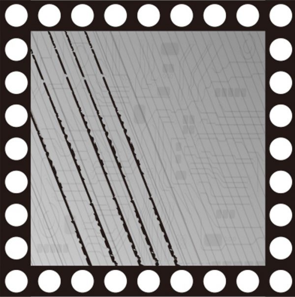
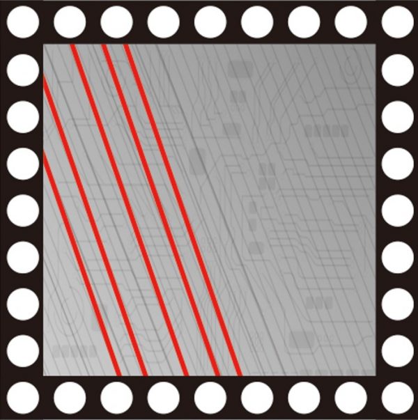
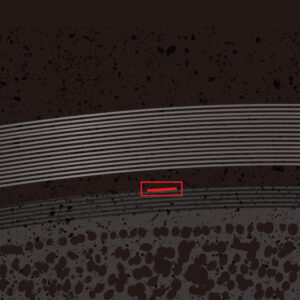
Defects caused by CMP usually include fine scratches, particle residue, and polishing pad debris. After polishing, the wafer will generate extremely shallow polishing traces that form a complex background in inspection images. Because the types and positions of various defects are not fixed, they cannot be easily recognized. Other common surface defects such as white stains, black stains, water marks, and bubbles, are diverse and have no distinguishable or standardized features. Logic-based rules and algorithms of traditional systems are insufficient for effective inspection of an entire wafer.
AI powered defect detection
Using SolVision’s Segmentation tool, minute defects such as fine scratches can be located and marked on sample images to train the AI model. Even in complex or busy backgrounds, SolVision makes these obscure production flaws and their features visible, and can quickly identify their location and size for improved inspections.
AI Inspection
Scratched Surface