SolVisionCase Study
Quality Control of Wafer Dicing
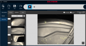
AI inspection of dicing blade defects
Quality of wafer dicing blades and tools
The rapid development of modern electronic products has intensified the demand and quality requirements for semiconductor chips. Advancements in manufacturing technology have also made silicon wafers become lighter, thinner and shorter. In order to achieve high yield and optimize production throughput, wafer dicing and singulation techniques are an important aspect to monitor, and the key to dicing quality lies in the blade used and its control.
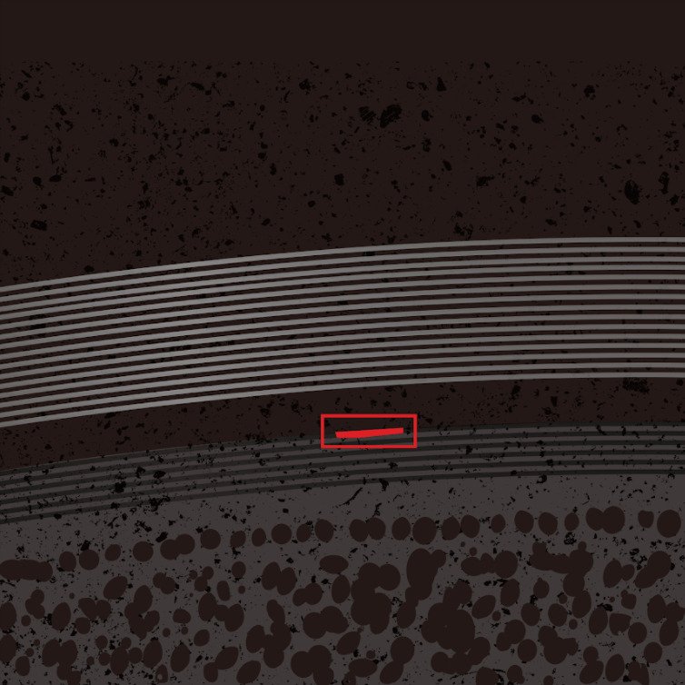
Circular blade patterns and complex backgrounds
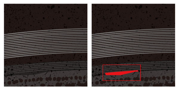
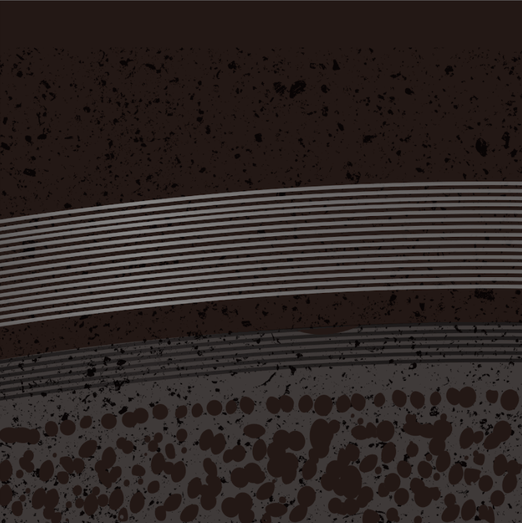
Wafer dicing is a common process in semiconductor and optoelectronic industries. When the dicing process cannot sustain yield and efficiency without compromising chip characteristics, production capacity will be greatly affected. Quality control of wafer dicing blades is mainly conducted by inspecting for appearance deficiencies. Damaged blades often have irregular lines or multi drilling defects on its surface. The dense, ring-shaped patterns on dicing blades also form complex backgrounds that affect detection rates of traditional inspection systems.
AI-based visual inspections
Using SolVision’s Segmentation tool, irregular lines and multi-drilling defects are labeled in sample images to train the AI model. By leveraging powerful algorithms and advanced machine vision technology, SolVision can identify various defects on wafer dicing blades in real time to maintain their quality, without being affected by the complexity of backgrounds or defects.
AI Inspection
Scanned Image
Detection Result