SolVisionCase Study
Inspecting Ball Grid Array Soldering Defects with AI
Case
Efficient and Dependable Chip Packaging
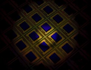
Ball grid array (BGA) technology is a favored packaging approach for advanced semiconductor chips, initially developed to address electrical shortage issues. This method involves arranging small solder balls on the chip’s bottom surface to decrease the packaging area and enhance reliability.
Manufacturers commonly employ plastic BGA, leveraging laminated substrates for a cost-effective solution. However, temperature variations during reflow soldering may occasionally deform the PCB and BGA, leading to non-wetting defects and solder ball overlap, resulting in short circuits.
Challenge
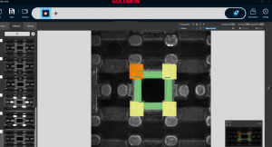
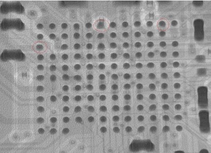
Reducing Noise and Enhancing Edge Visibility in X-ray Inspection of Soldered Joints
Traditional optical inspection methods are ineffective in verifying soldering quality for concentrated solder balls on the bottom surface. X-ray equipment becomes essential for penetrating and detecting potential false soldering. However, X-ray images often exhibit significant background noise and lack clear edges in grayscale, posing challenges for rule-based systems in analysis.
Solution
Enhancing X-ray Image Processing Through AI Acceleration
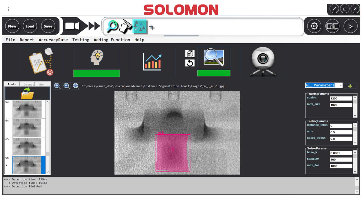
Leveraging deep learning, SolVision employs labeled sample images to teach the AI model the characteristics of false soldering defects in overlapped solder balls. Post-training, the AI model demonstrates accurate detection and recognition of various soldering defects, even in X-ray images characterized by noisy backgrounds and unclear edges.
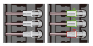
Defect Detection
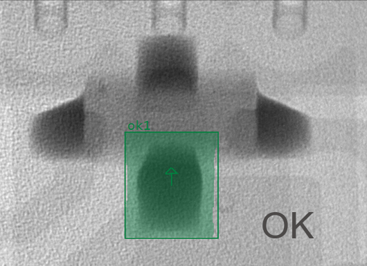
OK
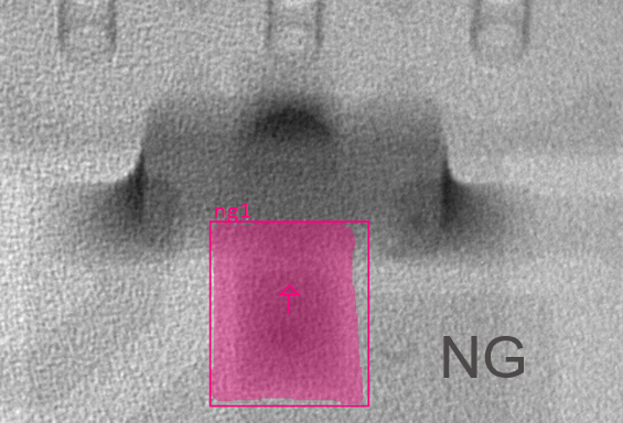
NG
Wrong size
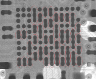
Short circuit