SolVisionCase Study
Inspecting Packaged Semiconductor Chips
AI unsupervised learning for detecting micro defects
External protection layer and packaging processes
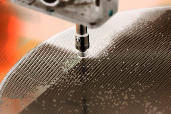
Cutting processes affect the quality of semiconductor wafers. Occasionally, defects such as surface cracks occur when wafers are singulated. After they are packaged, wafers are fastened to the protective plastic or ceramic packaging, making it hard to inspect for edge cracks or other internal micro defects using traditional methods.
Detecting through packaging
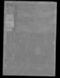
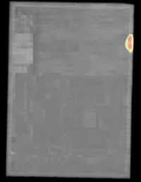
When inside its packaging, a wafer can only be photographed using a special light source and lenses with penetration properties. This creates images that show edge cracks and edges in very similar colors, making them difficult to distinguish. Additionally, the shape and angle of small cracks are irregular, so traditional rule-based systems are not effective for such inspection tasks.
Judging perfect and imperfect products
Powered by AI, Solvison offers individual functions designed to supplement different inspection tasks. The Anomaly Detection tool uses deep learning technology to teach the AI model sample images of “perfect” wafers. The data augmentation tool facilitates simulation of potential wafer deviations to expand the AI database of production scenarios and strengthen recognition ability. After training, the AI model can compare the golden sample with a scanned image to identify and locate defects such as micro cracks on the edge of a packaged chip, without being affected by imaging quality or near identical colors.
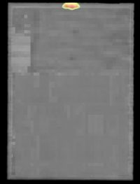
AI Inspection
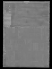
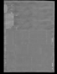
Scanned Image
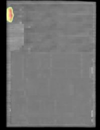
Detection Result