SolVisionCase Study
Visual Inspection of Semiconductor Carrier Trays
Automated defect detection with artificial intelligence
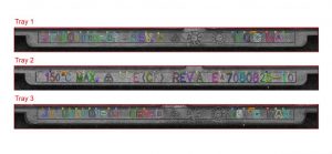
Stability and positioning of semiconductor trays
Semiconductor carrier trays are indispensable to semiconductor processing, and they come in different formats and material according to the application and environment. In addition to the safety and stability of chips, the position and picking points of trays need to match feed mechanisms precisely during production. The quality of the tray therefore reflects the success of production automation.
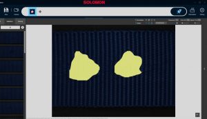
Inspecting complex backgrounds and obscure defects
The outline and positioning holes of carrier trays are prone to defects such as chipping and warping caused by production temperature and long-term usage. These trays were previously screened using traditional methods – yet due to their complex formats and the obscure, random nature of tray defects, implementing rule-based vision systems for visual inspection tasks often led to production yield and efficiency issues.
Overcoming the obstacles of traditional inspections
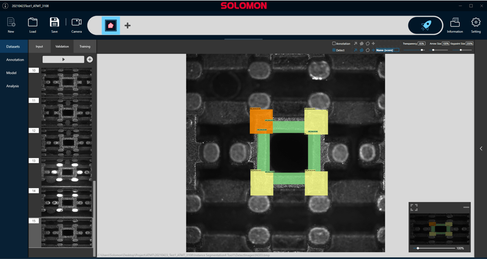
SolVision’s Segmentation tool is capable of recognizing defects by locating and labeling them, even in complex backgrounds, to monitor for production anomalies and be able to eliminate faulty trays in real time.
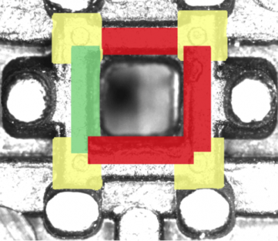
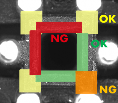
AI Inspection
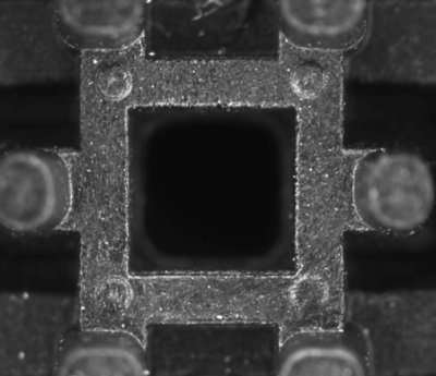
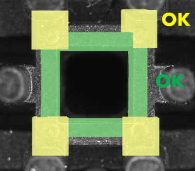
Complete inspection
Original
Result
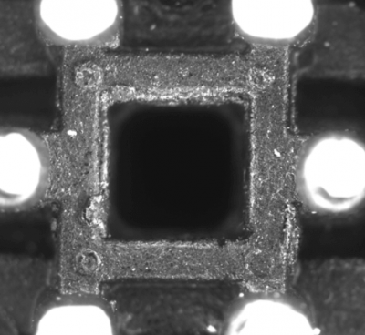
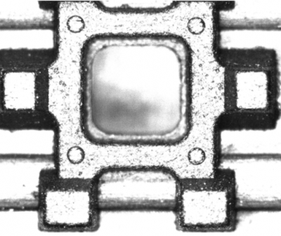
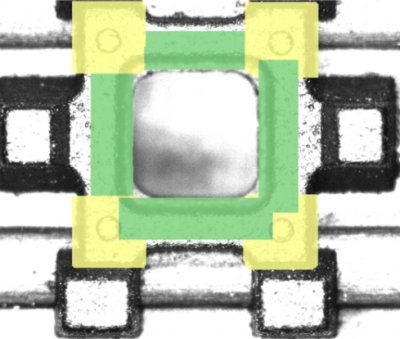
Positioning hole gaps and frame defects
Original
Result
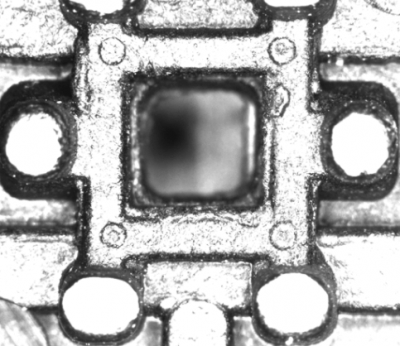
Complete inspection
Original
Result
Border defects
Original
Result