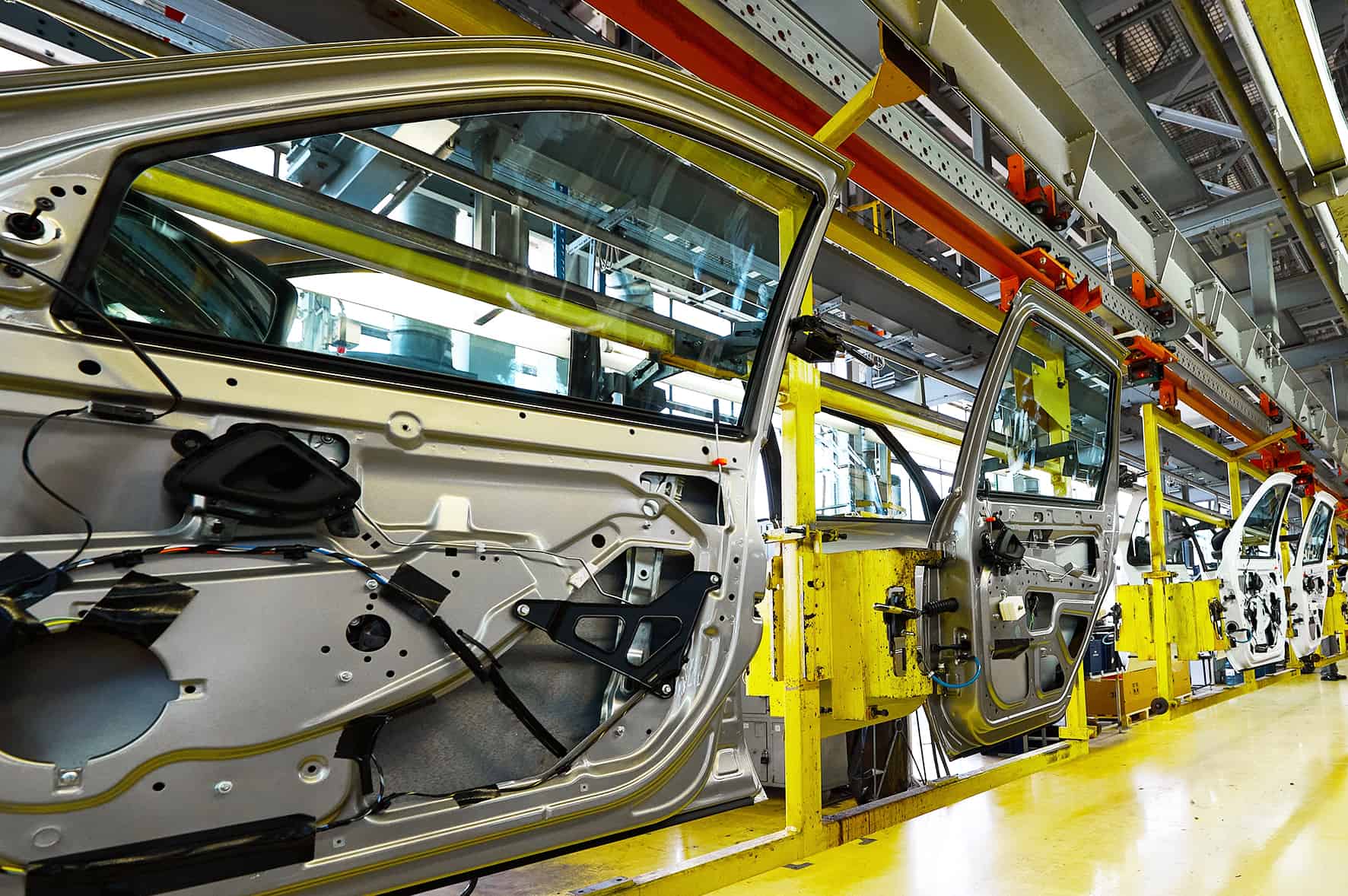
META-aivi optimizes automotive parts quality control with AI, reducing errors and digitizing the process for unparalleled product inspection efficiency.
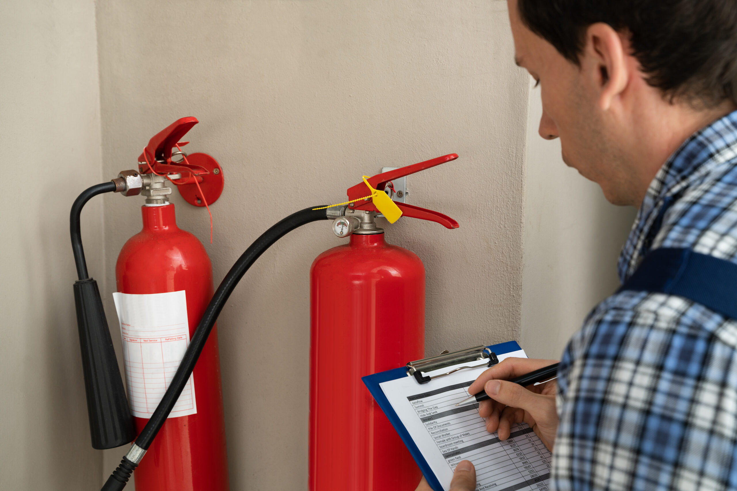
Discover how a company improved fire extinguisher inspections by implementing META-aivi, enabling real-time issue detection, streamlining processes, and reducing inspection time by 60%.
META-aivi enables real-time detection of foreign objects in food production, addressing challenges associated with manual inspection such as worker fatigue and the risk of human error.
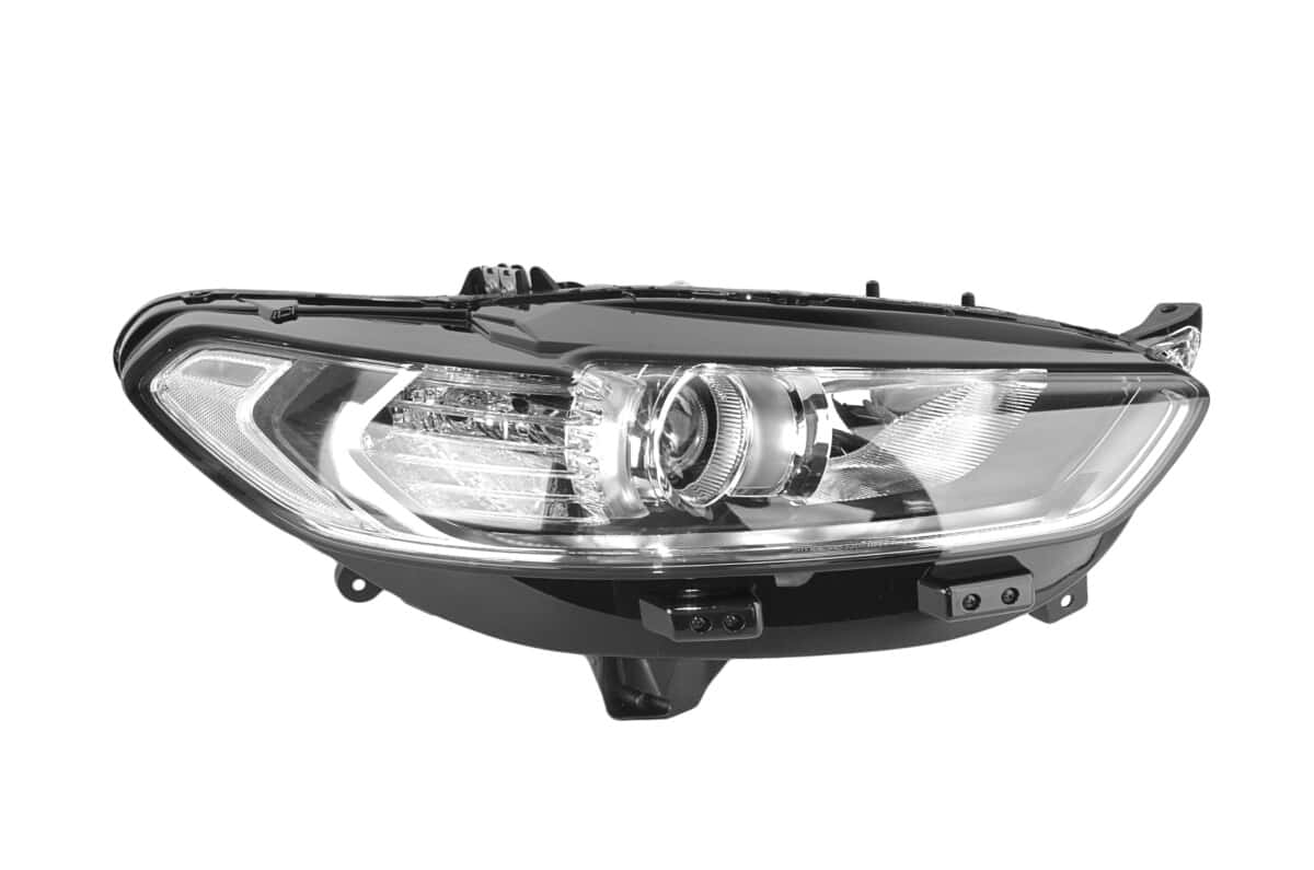
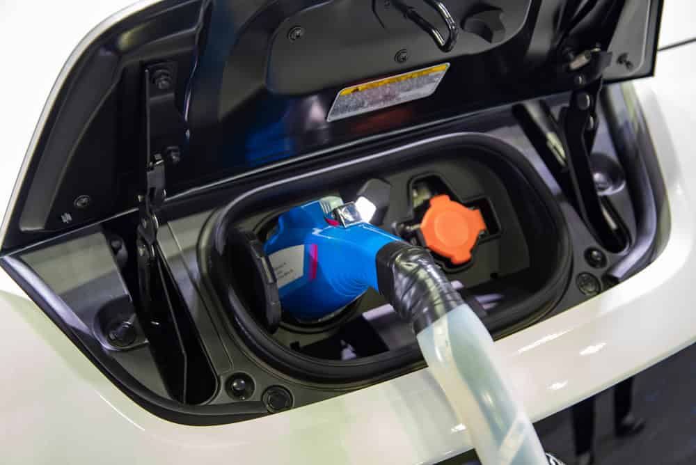
Discover how META-aivi’s AR + AI capabilities enhanced electric vehicle assembly verification and quality control for one of the world’s leading EV manufacturers.
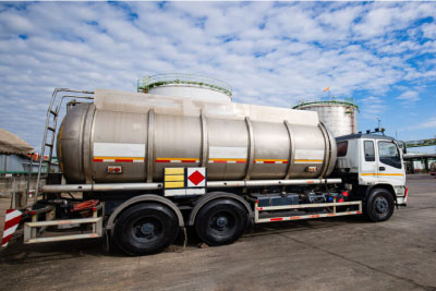
META-aivi uses AI detection to perform a step-by-step inspection of the chemical tanker loading/unloading process to ensure the operator is following the correct procedure.