solomonadmin

  • AI Inspection of Semiconductor Carrier Trays

    With SolVision’s Instance Segmentation tool, the various placement possibilities of chips on carrier trays can be learned by AI image processing.

  • Inspecting Packaged Semiconductor Chips

    The Anomaly Detection tool uses deep learning technology to teach the AI model sample images of “perfect” wafers.

  • a group of square objects

    Detecting Chipping Defects in Wafer Dicing

    The location, size and shape of cracks vary each time, and traditional optical inspection cannot accurately identify such unpredictable defects.

  • Quality Control of Wafer Dicing

    Using SolVision’s Instance Segmentation tool, irregular lines and multi-drilling defects are labeled in sample images to train the AI model.

  • AI Visual Identification and Classification of Cells

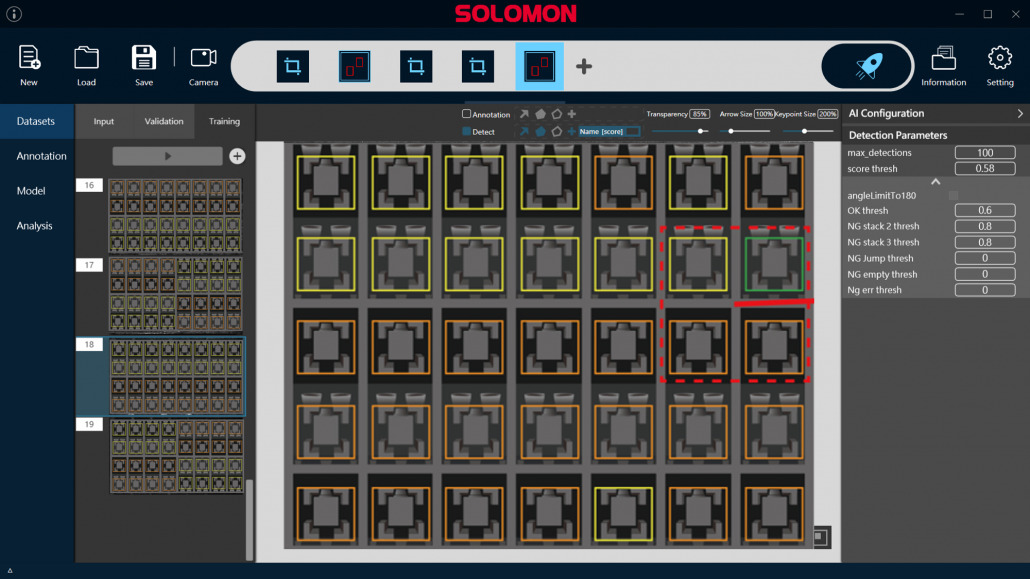
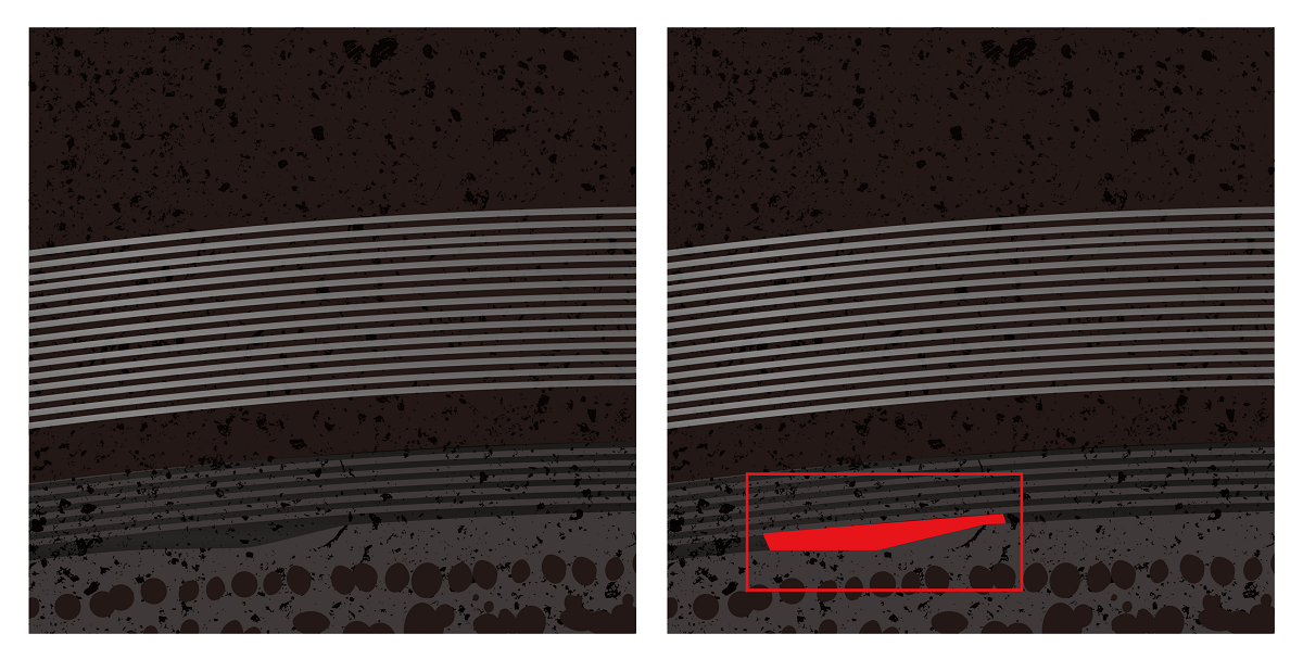
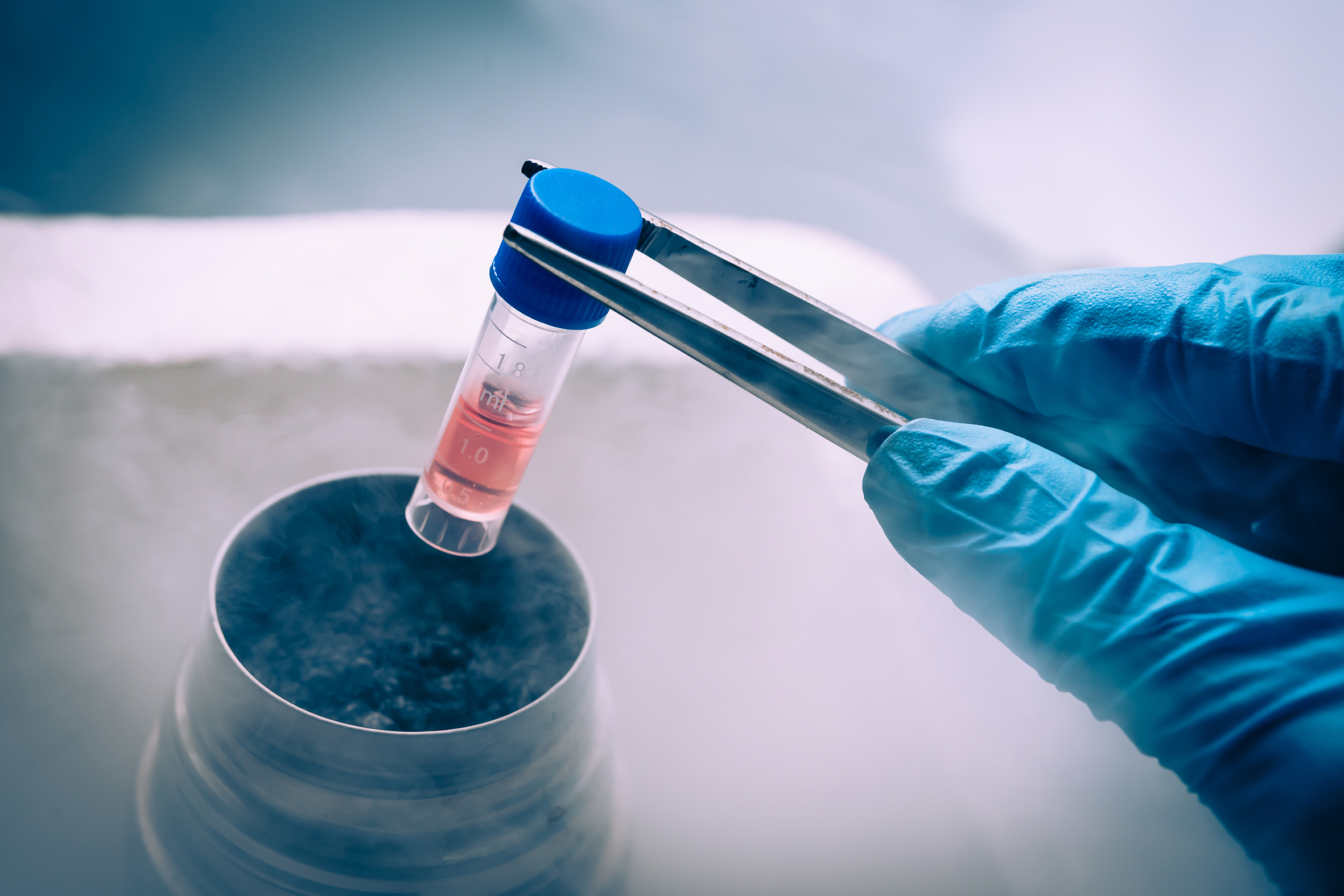
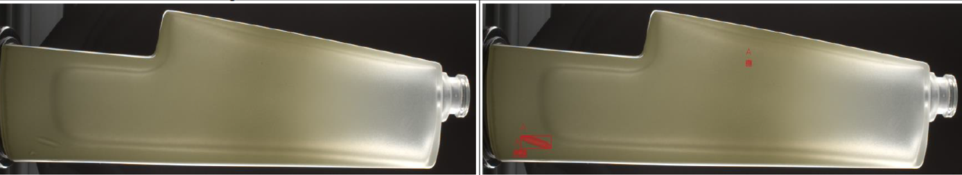
    Deploy SolVision’s advanced AI model to identify and classify cells where traditional AOI systems are insufficient in detecting and determining cell variations

  • Automating Inspection Processes for PCBs

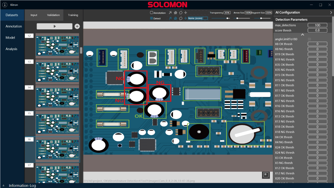
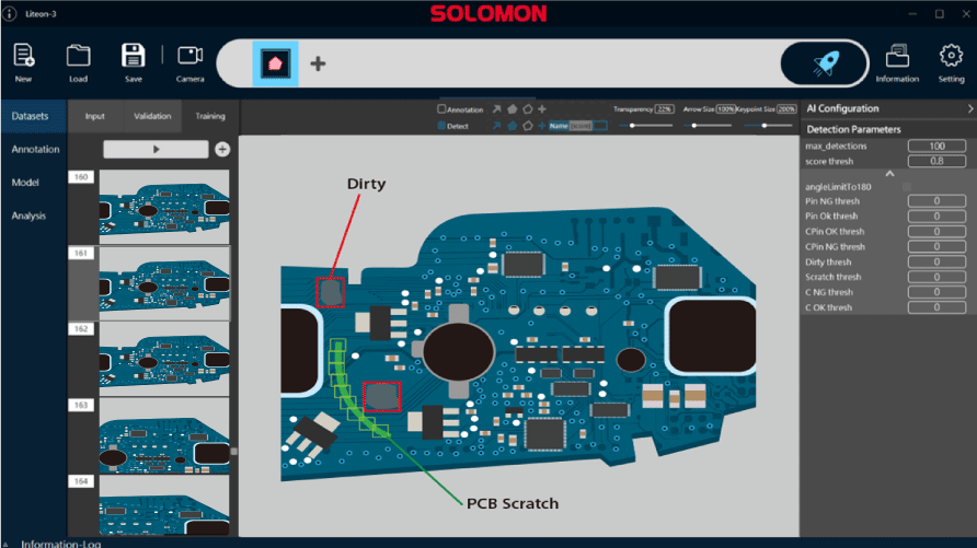
    SolVision first defines assembly characteristics of each component on the PCBA, then trains the AI model to recognize them via image processing to inspect for defective components.

  • Visual Inspection of Glass Bottles

    Through advanced image processing, SolVision can fully automate inspection processes to detect production flaws.

  • AI Inspection for Aluminum LEDs

    SolVision can locate and recognize the smallest defects and production anomalies on aluminum PCBAs through image processing.

  • Inspecting Packaging Seals

    Based on deep learning technology, SolVision can determine whether a seal is intact by comparing a perfect packaging with potential variations